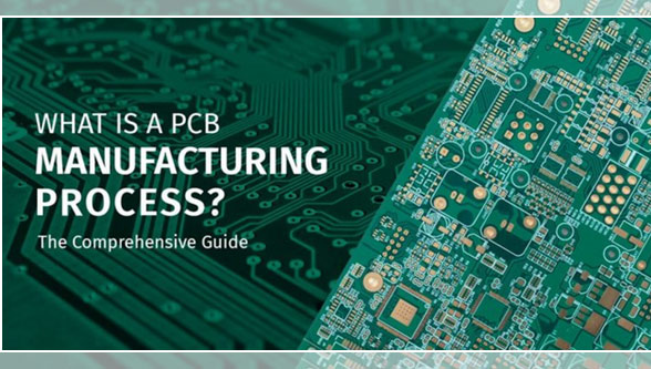
The whole PCB manufacturing process takes a complex path to ensure the performance of the final product. While there are various types of circuit boards, such as single, double, and multilayered PCBs, their manufacturing process only differs after the fabrication of the first layer. Because of the differences in circuit board designs, some PCBs have more than 18 manufacturing steps.
Step 1: Designing the PCB
The initial step of the PCB manufacturing process is the design or plan of the task ahead. Here, the designer outlays a sketch for the circuit board that meets the application requirements. The manufacturer then checks the design through the Design for Manufacturability (DFM) process to ensure that it meets the tolerances required for fabrication.
Step 2: Design Review and Engineering Questions
The second step of the PCB manufacturing process involves examining the design for potential faults. After the engineer is satisfied with the design outlay, he forwards it to the printing stage.
Step 3: Printing the PCB Design
Unlike other standard designs, such as construction designs, circuit board designs are not printed on an ordinary paper. Instead, PCB manufacturers use a special type of printer – plotter printer – to print PCB designs. This printer basically creates a “film” of the circuit design – an image negative of the design.
Step 4: Printing Copper for the External Layers
After printing the design, the manufacturer pre-bonds copper laminates to act as the structure of the circuit board. Secondly, they etch away excess copper to expose the design. Thirdly, they cover the laminate panel with a photo-sensitive film known as a resist.
Step 5: Etching the Inner Layers to Remove Copper

The PCB manufacturer needs to remove any extra copper from the internal layers before proceeding with the PCB manufacturing process. Etching entails extracting any unprotected copper from the board. This step varies from board to board.
Step 6: Layer Alignment


After etching all the inner layers, they need to be aligned for optical inspection. Still, the engineers use the registration holes they created in step three to align the internal and external layers. To achieve this, the engineer places the boards on an optical punching machine, which punches a pin via the registration holes, aligning the PCB layers.
Step 7: Automated Optical Inspection (AOI)


After layer alignment, the technician conducts an automated optical inspection to ensure there are no faults. This step is vital since once the layers are stacked together, any existing defect cannot be solved. This ensures no errors, and an AOI equipment compares the board with the Gerber file design, which acts as the manufacturing model.
Step 8: Laminating the PCB Layers
The circuit board lamination process comprises the layup and laminating steps. The external PCB surface consists of fiberglass pieces pre-soaked with an epoxy resin. On the other hand, the inner parts consist of a thin copper foil with copper trace etchings. When these two parts are ready, they are fused.
Step 9: Drilling
First, the technician uses an X-ray machine to establish the drill spots. Then, they create registration holes to secure the stack before drilling more specific holes. They use an automatic drill to create the holes using the Gerber file as a manual. Upon completion of this step, any extra copper found at the PCB edges is removed.
Step 10: Plating
The PCB plating process applies a chemical to fuse the layers. After a thorough cleaning, the board is dipped in different chemicals to coat the PCB panels in a micron-dense layer. The coat is applied on the outer layer and into the apertures.
Step 11: Outer Layer Imaging
The PCB manufacturing process comprises two photoresist applications. The first one is applied in step four and the second one in step eleven. However, the second photoresist application is done on the external layer because it is the only one that requires imaging..
Step 12: Outer Layer Etching
Manufacturers remove all the unwanted copper and resist coating to prepare the external layer for AOI and solder masking.
Step 13: Outer Layer AOI
Like the internal layer, the external layer must go through the AOI process. The process ensures the layer is up to the specified design requirements. Besides, it verifies that the outer layer etching process eliminated all the unwanted copper to make a high-quality board.
Step 14: Solder Mask Application
PCB panels should be thoroughly cleaned before applying a solder mask. After cleaning, they are exposed to UV light to establish where to remove the solder mask. Once the engineers remove the mask, they place the PCB in an oven to cure.
Step 15: Silkscreen Application
Since circuit boards should have labels, manufacturers print essential information on the board surfaces by applying silkscreen. This information may include company identification, warning labels, logos, component numbers, pin locators, and others.
Step 16: Finishing the PCB
This step involves plating with conductive materials, like:
Immersion silver: This method offers minimal signal loss, it’s free from lead compounds, and adheres to the RoHS standards.
Hard gold: This surface finish method is durable, follows the RoHS standards, and does not contain the lead compound.
Electroless nickel immersion gold (ENIG): ENIG is a popular surface finish method that is durable and follows the RoHS standards.
Hot air solder leveling (HASL): This method is cheap, durable, and reworkable.
Lead-free HASL: is cost-effective, free from lead, follows the RoHS standards and is reworkable.
Immersion tin (ISn): is mainly applied in press-fit use cases, tight aperture tolerances, and tin whiskers.
Step 17: Quality Check and Visual Inspection
Before manufactures package their PCB products, they pass them through a final quality inspection process that confirms:
- The aperture size is uniform on all the PCB layers and is up to the design specifications.
- The PCB dimensions match the design specifications.
- The PCBs are free of dust and any other contaminants.
- The finished PCBs do not have burrs or sharp border points.
Conclusion
The discussion above clearly shows that a lot of effort is put into the PCB manufacturing process. Learning the complexities of this process and the function of each step gives you a better appreciation of the cost, commitment, and time invested in creating a circuit board. To ensure your PCB designs are manufactured to precision, you must partner with a reputable manufacturer who emphasizes quality over anything else.
Article by – Linda Liu
Linda Liu is the overseas marketing manager for MKTPCB, a leading PCB manufacturer that offers high-quality PCB products and services. Since 2012, she has established “first-of-its-kind” industry-changing and transformational businesses initiatives that increased revenue growth, brand exposure and market expansion for MKTPCB. Linda graduated from Western University with a bachelors degree in marketing.